Pulled out the dremel, made room on the kitchen table, got the bits ready...
Tonight I drilled, tinned, and soldered in the components for the small solid state preamp section that is intended to go into the tube amp, as its own channel.
I designed and drew up the PCB layout myself in Protel a while back. The first revision I had (which was posted earlier in the blog) was incorrect. I had the pinout for the J201 junction field-effect transistor (jfet) wrong.
The PCB was made using a precoated, positive photoresist type blank board and a transparent layout of the circuit traces. The transparency was placed on the blank pcb and light was exposed onto the transparency. Any space on the PCB that had light hitting it would be a section of copper that would later be removed. Because the circuit traces were printed in black, no light hit the PCB at those places. After exposing the board, it was placed into a developing solution to remove the coating the resists the etchant later used to remove the unwanted copper. After developing the board it was placed into yet another solution of diluted hydrochloric acid, made from muriatic acid and hydrogen peroxide. I shall not go into the specifics for making this solution. I do not wish to be held responsible for someone burning themselves or others. Google it, if you're interested.
With the etched board it was time to drill the holes. I used a Dremel rotary tool sitting in a press specifically made for it, and some cheap Harbor Freight miniature drill bits. For most of the holes I used a 0.0256in drill bit, and bored out some to 0.0330in as needed. This setup is not perfect. I noticed some heavy pivoting action going on at the drill bit, probably because of the weak tolerances of every part I am using, from the Dremel to the aforementioned "cheap" Harbor Freight bits.
After drilling and tinning the pcb, I began populating the board. Everything went smoothly. The time I had spent so tediously measuring the component leg spacing paid off. I'll have to admit as well, the photography is not half bad...
After drilling and tinning the pcb, I began populating the board. Everything went smoothly. The time I had spent so tediously measuring the component leg spacing paid off. I'll have to admit as well, the photography is not half bad...
Here are some pics of the process, beginning from the drilling stage:


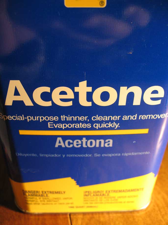
A bit of acetone to remove the resist coating of the pcb. And a bit of magic tinning solution. This stuff is awesome!


7:40PM - 11:30PM (3.83HRS)
No comments:
Post a Comment