Search This Blog

Tuesday, November 30, 2010

More Metal Work - Fabrication

Just when I thought all the metal shavings were cleaned up, I noticed I forgot to drill some holes:
  • Power Switch
  • Fuse holder
  • AC inlet (grommet/strain relief)
  • Speaker output (1/4" female mono)
  • mounting holes for circuit boards
All of the above just happen to be somewhat important to the overall project. I had to drill some holes for the wiring entering the chassis, so I took advantage of the time to drill all the other holes needed. I am fairly certain that I have (NOW) taken care of any holes or metalwork that need to be attended to. As I type this, the cleaned panels and chassis are drying - I intend to cover them with a quick coat of flat paint, just to make the project look more homogeneous.

While drilling the last of the holes, I marked and drilled holes for an extra power transformer, if needed, to supply extra current for the tube filaments. I am uncertain that the power transformer I have will be adequate for all the tubes in the circuit. Tomorrow I will wire all the heaters up and do a quick test of any voltage drops/excess current. I have spare tube sockets that will allow me to perform this test.

Here are some pictures of tonight's mess:


5PM-9:15PM (4.5HRS)

O/P Xfmr measurements, CAD layout, chassis work, board building

Been busy since my last post.

Populated the main circuit turret board, components not yet soldered in.
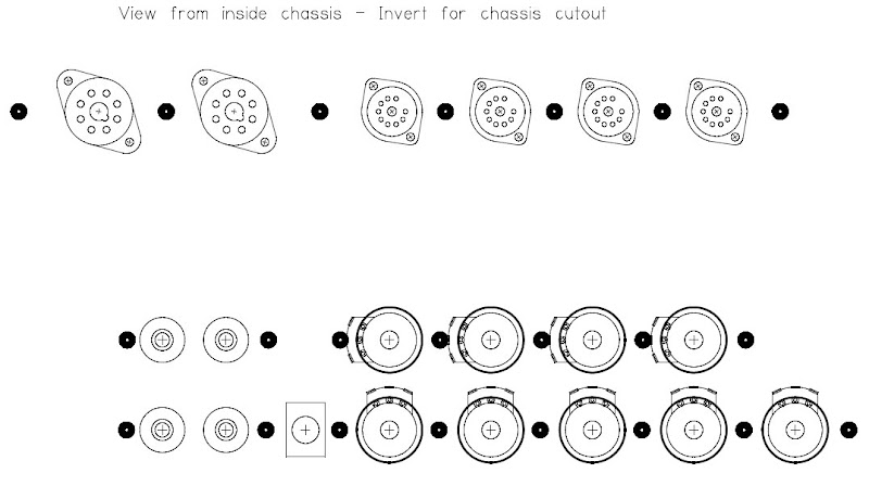


METAL WORK
  • drilled all holes for front panel components (pots, switches, jacks, etc.)
  • aligned and drilled holes for placement of front panel
    • countersunk philips head screws bolted to main chassis
  • punched out holes for tube sockets
    • re-drilled to compensate for existing ventilation holes
  • removed bulk metal from section of main chassis behind front panel
    • there is a gap between the two pieces of metal because of the way the chassis box was manufactured
  • laid out and marked chassis for transformers and capacitor board
    • need to drill before placement of main circuit board


I used CADStd again to assist in drawing out the placement of controls and tube socket layout. It makes it easier to place components when you can work with a 1:1 drawing and move them as needed, knowing that the dimensions do not change.


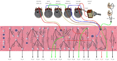
CAPACITOR EYELET BOARD

I did, however, use good old graph paper for laying out the capacitor bank board and the main rectifier diode board. Much faster.


The method I am using for these boards is similar to what Fender used in their original tube guitar amps. A layered board system with components on the top board, and the bottom one used as insulation. This way, the board can be mounted directly to the chassis without standoffs, and without danger of shorting out.


The metal holes that the components are placed into are called "eyelets". I was able to mount about half of the eyelets when the staking tool broke. I resorted to shortening the eyelets and using brute force to expand the eyelets once in their holes. The 1/8" holes that hold the eyelets were made with a hand whitney punch. There's no comparison for getting a job done using the right tool for the job. An example is most of the work I am doing now - I am trying to reuse old parts in an attempt to be "green" and to save money. A lot of the work done thus far could have been completed much faster with all the money in the world, and all the tools that go into said money.

I digress...

The capacitor board and diode board were then populated without soldering.

I also twisted some stranded insulated copper wiring for the tube filament wiring: Here is the method I chose to twist the wire:
  • place the 2 wires in a drill chuck
  • clamp the end of the 2 wires in a vise
  • holding the wire taut, activate the drill, spinning the wires
  • after the wires are sufficiently twisted, remove from drill and vise
Some thoughts on the latest work.
Metalwork is very messy. My garage workspace is now littered with metal shavings. It is also dangerous. I have had enough scrapes in the past to know how to do the work that I am doing without too much injury.


OUTPUT TRANSFORMER

Before mounting the output transformer I wanted to be sure the wire connections that I intend to make would be the correct ones. I took the transformer to school and ran a 1kHz sine wave signal into a wire I was absolutely sure (and later would be verified) was a speaker connection (secondary). I took the following steps:
  • measure input voltage
  • measure output voltage
  • calculate voltage ratio
  • SQUARE both sides (impedance ratio)
  • multiply both sides by expected speaker impedance
My calculations verified the proper wire connections to make (note I had extended the original wiring). This also confirmed the "thought" around the web that this particular transformer has a primary impedance of roughly 6k-OHMS.


NEXT STEPS
  • drill transformer mounting holes
  • drill/mark placement for power switch
  • drill/mark placement for RCA reverb connections
  • drill/mark placement for main circuit board
  • fabricate standoffs for boards

OVER 3 DAYS (16 HRS)

Monday, November 22, 2010

Transformer Mounts and Bias Circuits

This weekend I worked on the following:
  • power transformer chassis mounts
    • fabricated from angled aluminum stock I picked up at the local metal supply (Blue Collar Supply)
The power transformer I intend to use for this project is meant to be mounted semi-flush with the chassis. In it's stock form, a rectangular shaped hole is meant to be made to allow the bell-end of the transformer casing to fit into, and the transformer laminations rest on the chassis. I do not particularly enjoy metal work, probably mostly because I do not posses the tools to easily manipulate the pieces. I decided to fabricate some mounts for the transformer, so I can escape machining a large hole in the chassis. This way, I only have to drill 4 holes for mounting, and cut some angled aluminum. It went quite well.


I haven't made the holes for mounting yet. I plan to draw up a simple outline in CADSTD to have a visual size representation to work with on the chassis.


  • Output tube bias circuit
    • Adjustable, negative voltage power supply, full wave bridge, PI filter into 2 sealed trim potentiometers
On the turret board layout I made, I kept the output tube grid supply resistors on separate lines, with the intention that I should have provisions for separate bias supplies, to allow for compensation for mismatched tubes. I began with a voltage doubler circuit that I ended up not using, because the range of voltages was much too negative than I needed for the Fisher output stage. According to the 500-C schematic, the bias voltage in stock form is a set -17 V. I was getting anywhere from -40V to -102V DC from the first circuit.


I started over with a full wave bridge rectified power supply, grounding the positive side of the bridge. With this circuit I was able to obtain a range of -13V to -35V DC. I will have to recheck when the amp is powered up, as there was no other load on the power transformer.


I used a variable AC power transformer to "ramp" up the primary of the transformer that fed the power supply circuit. I did this because I am using old capacitors (from an old tube oscilloscope) and wanted to make sure I did not damage the electrolytic capacitors.


Here are some pics of the second version bias circuit:


  • Output Transformer wiring
    • Extended the wiring for the output transformer
Because the output transformer I am using is an old, used unit, the wires were somewhat shorter than I would like to work with. I found some spare wire and extended the existing wiring. I had to open up the transformer casing and expose the wires connected to the core.


  • Recycled some parts
    • I have some old terminal strip boards from previous junk-yard sales and such, and decided to put them to use. I desoldered all the old wiring/component residue from them and cleaned them up. Good as 60 years ago!


(8HRS)

Thursday, November 18, 2010

Editing layout - added control section

Added control section to layout, picked up a couple packs of 100k resistors, and 2 SPST toggle switches from the local shop, Metro Electronics. Also tested a possible candidate for the power supply choke (inductor) - measured at school with an LCR meter. Measured 3.3H @ 1kHz.


6PM - 9PM (3HRS)

Monday, November 15, 2010

Board Layout - Tube Pin Connections

Worked on layout - drawing wire connections to be made from board to tube socket pins. Found a clever way to draw a smooth curved line in Photoshop (http://www.agavegroup.com/?p=68).


8:00PM-10:00PM (2HRS)

Sunday, November 14, 2010

Board Component Overlay

Confirmed board layout before cleaning board/installing components. Created layout on PC to use a guide.


To do:

  • Get extra 100k resistors (missing a few)
  • Draw up wiring guide/confirm connections
  • Decide on bias circuitry
  • Clean up used tube sockets (remove old solder)
  • Extend wiring for O/P XFMR
(2.5HRS)

Thursday, November 11, 2010

Making the Solid State preamp stage PCBs

Pulled out the dremel, made room on the kitchen table, got the bits ready...

Tonight I drilled, tinned, and soldered in the components for the small solid state preamp section that is intended to go into the tube amp, as its own channel.

I designed and drew up the PCB layout myself in Protel a while back. The first revision I had (which was posted earlier in the blog) was incorrect. I had the pinout for the J201 junction field-effect transistor (jfet) wrong.

The PCB was made using a precoated, positive photoresist type blank board and a transparent layout of the circuit traces. The transparency was placed on the blank pcb and light was exposed onto the transparency. Any space on the PCB that had light hitting it would be a section of copper that would later be removed. Because the circuit traces were printed in black, no light hit the PCB at those places. After exposing the board, it was placed into a developing solution to remove the coating the resists the etchant later used to remove the unwanted copper. After developing the board it was placed into yet another solution of diluted hydrochloric acid, made from muriatic acid and hydrogen peroxide. I shall not go into the specifics for making this solution. I do not wish to be held responsible for someone burning themselves or others. Google it, if you're interested.

With the etched board it was time to drill the holes. I used a Dremel rotary tool sitting in a press specifically made for it, and some cheap Harbor Freight miniature drill bits. For most of the holes I used a 0.0256in drill bit, and bored out some to 0.0330in as needed. This setup is not perfect. I noticed some heavy pivoting action going on at the drill bit, probably because of the weak tolerances of every part I am using, from the Dremel to the aforementioned "cheap" Harbor Freight bits.

After drilling and tinning the pcb, I began populating the board. Everything went smoothly. The time I had spent so tediously measuring the component leg spacing paid off. I'll have to admit as well, the photography is not half bad...

Here are some pics of the process, beginning from the drilling stage:


A bit of acetone to remove the resist coating of the pcb. And a bit of magic tinning solution. This stuff is awesome!


7:40PM - 11:30PM (3.83HRS)

Friday, November 5, 2010

Solid State Gain

Another thought - I might need an extra gain stage between the output of the solid state preamp and the phase inverter. I plugged a "pedal" version of the anticipated preamp into a tube power amp and noticed somewhat low volume, as well as noise, showing up as hum on the output. Perhaps some kind of impedance matching is necessary. I will consider this while preparing the amplifier, and hopefully be ready to implement something if necessary.

(0.5HRS)

Mounting turrets

Today I went to school and used the heavy duty drill press they have in the lab and drilled all the holes (1/8" diameter) for the turrets, and holes for wire routing. The fiberglass board that I drilled into was quite nice to work with, albeit a bit of a dust maker. **Always wear eye and respiratory protection when cutting fiberglass** I think I was expecting similar results to PCB material, but then I believe that those are more densely packed fiberglass and a different type of epoxy to hold it all together.

I covered the board with tape and marked lines for the cutouts, center-punched the soon-to-be holes and drilled away.

Once the holes were drilled I removed the tape and cleaned up the board. Now came the task of mounting the turrets. I was missing the bit that sits in the press and pushes the top of the turret against the board, while the conical section flares the bottom. I had a standoff that I bored out with a 5/32" bit. That fit the turret head pretty good and I did the same thing to a longer metal hex standoff and pressed in the turrets.


Next step - mounting the components. I'll have to find some chassis mount terminal strips to mount the other components (diode rectifiers, bias circuit, etc...)

3 HRS CLOCKED - 1 HR @ HOME